Surface optimization in semiconductor frontend and backend processes
Wettability – Adhesion – Surface Tension – Foam Prevention
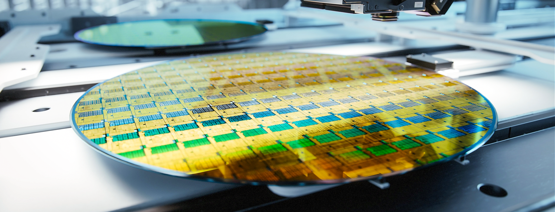
In hardly any other industry are the quality requirements as high as in semiconductors, where the countless steps from the raw wafer to the encapsulated chip are permanently optimized and quality-checked. Surface science serves to investigate the interface processes associated with almost every frontend and backend step to ensure cleanliness, wettability, and adhesion wherever necessary.
Frontend processes
From the raw wafer cut from the silicon crystal (ingot) to the finished wafer ready for chip production, several surface treatment and cleaning steps are involved. Tensiometers, contact angle instruments, and foam analyzers support R&D departments in these processes and help in QC to provide for wafers of the highest quality and the lowest possible reject rate.
Wafer planarization
In chemical-mechanical planarization (CMP), surfactants ensure an optimally mixed slurry and good wetting by lowering the surface tension. Both can be quantified with a tensiometer. To counteract undesirable foaming, the foaming behavior of the slurry is investigated.
Wafer cleanliness
The contact angle (CA) reacts strongly to contamination or to cleaner residues. Therefore, the CA is an ideal test parameter for the optimization and QC of the various front-end cleaning steps. Testing with pure water, the wafer’s quality is not impaired.
Automated batch testing
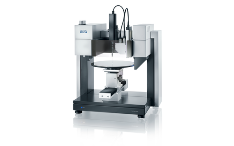
For series QC checks for cleanliness or wettability, mobile contact angle instruments are combined with robotic systems, while their software seamlessly communicates with the surrounding system using an API or the OPC UA protocol.
Backend processes
The steps for mounting and protecting the finished chip (packaging) involves several interfacial contacts for which surfaces must be prepared and quality-checked to ensure good wetting and adhesion. For measuring the quantities involved and for analyzing surfaces of different size ranges down to tiny bond pads, a range of instruments for surface analysis is available.
Die underfilling
When underfilling the chip with epoxy resin, wetting must be optimal so that every position is quickly reached and no air pockets remain. Contact angle measurements support packaging engineers in this respect and even enable calculating the spreading speed.
Wire bonding
To ensure excellent conductivity and mechanical stability when wiring the chip, the bond pads must not be contaminated or oxidized. The contact angle provides important information for surface optimization. These analyses are carried out using special micro equipment for measuring with picoliter drops.
Glob top encapsulation
The resin coating around sensitive components must provide long-term protection, e.g. against moisture or mechanical stress. Contact angle measurements enable determining adhesion and interfacial tension, which is decisive for long-term stability.


